
Hardware Architecture & Precision PCB Design
From initial system architecture and schematic capture to high-density multi-layer PCB layout and DFM validation. We design reliable hardware engineered to pass EMC and operate continuously under extreme load.
PCB Engineering
Hardware Design Capabilities
Schematic Capture & Component Selection
Selecting components optimized for availability, temperature ratings, lifecycle longevity, and BOM cost. Robust power trees and ESD protection.
Multi-Layer High-Speed PCB Layout
4 to 12+ layer stackups with controlled impedance routing (USB 2.0/3.0, Ethernet MII/RMII, DDR/Flash, RF coplanar waveguides).
Power Distribution Network (PDN)
Low-noise switching regulators, linear LDOs, battery management systems (BMS), decoupled power planes, and transient voltage suppression.
EMC/EMI Pre-Compliance Design
Ground plane partitioning, continuous return paths, shielding cans, ferrites, and layout techniques to pass CE, FCC, and industrial EMC certifications.
Signal Integrity & Thermal Dissipation
Length matching, differential pair tuning, thermal vias, heat spreader design, and board temperature modeling under peak microcontroller workloads.
Design for Manufacturing & Test (DFM/DFT)
SMT pick-and-place optimization, panelization, test-point allocation for ICT/boundary scan, and turnkey Gerber/drill/BOM package generation.
EDA Toolchains
EDA Platforms & Manufacturing Handoff
We work seamlessly in modern electronic CAD environments including Altium Designer, KiCad, and Cadence OrCAD. Every hardware release is accompanied by comprehensive manufacturing documentation:
- ❯ Production Gerber (RS-274X / ODB++) files
- ❯ Excellon NC drill files with slot definitions
- ❯ Bill of Materials (BOM) with manufacturer part numbers & second-source alternates
- ❯ SMT Pick-and-Place (Centroid) XY coordinates
- ❯ 3D STEP models for mechanical enclosure clearance checking
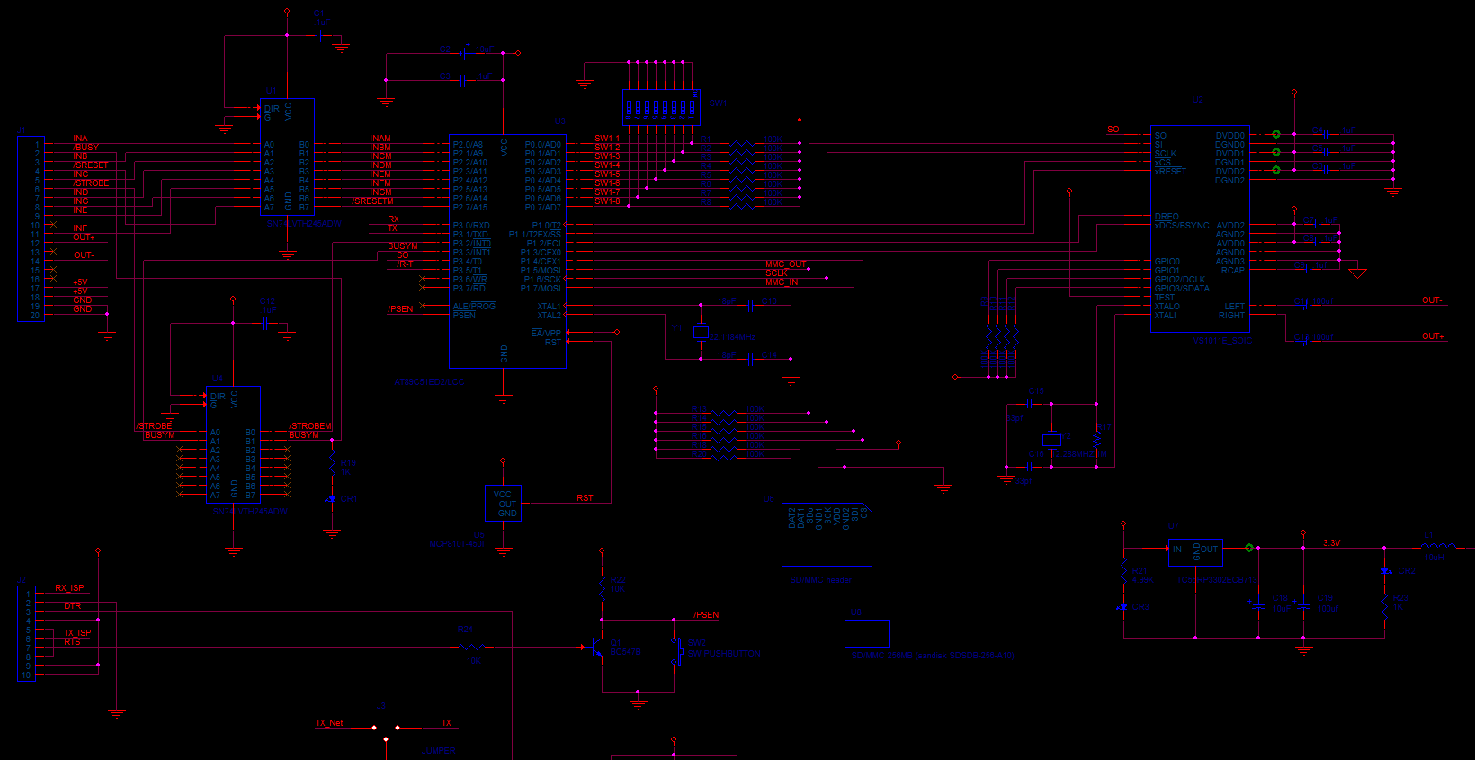
Production Schematic Capture — Mixed-Signal MCU & Audio Subsystem